Sign in
Menu
Sign in

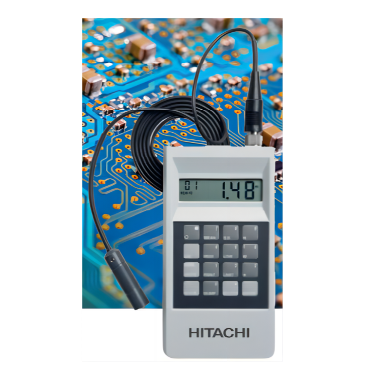
Hitachi ETP Probe

2 year ago
51 0
Product details

PTH hole copper (Hitachi ETP Probe) test principle
Measured by the principle of eddy current, the ETP probe has a probe, the probe is composed of two coils,
when measuring, one of the coils emits electromagnetic field, the free electrons inside the conductor do circular motion in the electromagnetic field, generating a cyclotron current (eddy current), the eddy current generates an electromagnetic field in the direction opposite to the electromagnetic field generated by the coil, received by the other coil. An electrical signal is generated, and the thickness of the hole copper is measured due to the different thickness of the hole copper and the different size of the signal. It can be seen that the electrical conductivity of the metal is different, and the strength of the electrical signal is different, so the measured thickness is not the same.
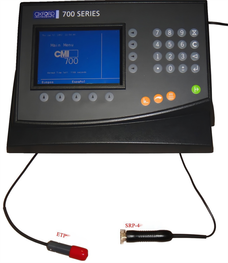
ETP Probe
 
Hitachi ETP Probe's Five Core Advantages
 
1. High Precision: Micron-level measurement, suitable for high-frequency/high-speed PCBs
Resolution: 0.1μm, accurately distinguishing copper thickness differences as small as 1μm, meeting the stringent requirements of 5G base station PCBs (via copper thickness ≥ 20μm ± 2μm) and high-speed server PCBs (surface copper thickness control accuracy ±1μm);
Linearity: Within the 5-50μm range, the output signal (impedance change) exhibits a strict linear relationship with copper thickness (R² > 0.999), eliminating nonlinear errors in low-thickness areas (<10μm);
Repeatability: Single-point measurement standard deviation < 0.3μm, and R&R (Repeatability and Reproducibility) < 5% for 10 measurements, far exceeding the IPC-TM-650 standard (≤ 10%), ensuring consistent quality across the production line.
 
2. Non-contact Inspection: Avoids Mechanical Damage and Chemical Contamination
No physical contact: The probe maintains a distance of 0.1-1mm between the probe and the copper layer. Inspection is completed through electromagnetic field coupling, completely eliminating the scratches on the copper layer caused by pressure from traditional mechanical probes (especially suitable for flexible printed circuits (FPCs)).
Chemical Corrosion Resistance: No chemical reagents are involved in the inspection process, preventing the probe from corroding chemicals such as flux and cleaning agents, extending the maintenance cycle to 3 months.
Long Life: No wearing parts, the probe lifespan exceeds 500,000 measurements, reducing maintenance costs by 90%.
 
3. Multi-band Adaptive Frequency: Covers the Full Thickness Range
Low-frequency mode (1-10MHz): High penetration depth (up to 50μm), suitable for inspecting thick copper layers (e.g., power supply boards >35μm), avoiding excessive attenuation of high-frequency signals in thick copper.
High-frequency mode (10-100MHz): High resolution (<0.1μm), suitable for inspecting thin copper layers (e.g., high-frequency boards 5-15μm), accurately capturing subtle thickness variations.
Intelligent frequency switching: The probe's built-in frequency adaptive algorithm automatically switches to the optimal frequency based on copper layer thickness, allowing a single probe to cover the full thickness range of 5-50μm.
 
4. Fast Testing: Single-hole measurement time <0.5 seconds
High-Speed Sampling: The coil impedance sampling frequency reaches 100kHz, enabling real-time capture of eddy current decay curves (approximately 20ms);
Parallel Computing: The built-in DSP chip processes data in real time, achieving a 0.3-second transition from magnetic field excitation to thickness display, a five-fold improvement in efficiency compared to traditional eddy current probes (1-2 seconds);
Batch Testing: Combined with the CMI700's automatic scanning platform, it can achieve batch testing of 120 holes per minute, meeting the demands of online production line testing.
 
5. Strong Environmental Adaptability: Stable operation in complex working conditions
Temperature Compensation: The built-in NTC thermistor automatically corrects for the effects of ambient temperature (10-40°C) on copper conductivity, ensuring consistent measurements at varying temperatures;
Electromagnetic Interference Resistance: The probe's shielded design (e.g., copper foil wrapped around the coil) protects against interference from strong electromagnetic fields found in production lines (e.g., reflow soldering equipment);
Low Humidity Tolerance: Stable operation in environments with a relative humidity of 20-90%, eliminating the signal drift associated with humidity fluctuations associated with traditional probes.
 

Technology data for ETP Probe:

Accuracy:

±0.01mil(0.25um)<1mil(25um)

Resolution:
0.01mils(0.25um)
Eddy Current:
comply with ASTM E37696 standard regulation
Testing thickness range:
0.08-4.0mils (2-102um)
Min hole dia:
35mils(899um)
Hole dia range:
0.899mm-3.0mm


III. Typical Application Scenarios
 
Semiconductor Substrate Production: Advanced Packaging High-Density Interconnect
In TSMC's CoWoS (Chip-on-Wafer-on-Substrate) substrate production, the Oxford ETP Probe is used for:
Blind Via Fill: Detecting the copper fill thickness inside laser blind vias (5μm diameter) to ensure the absence of voids or recesses (fill ratio >99%);
Any-Layer Interconnect: Measuring the thickness of inner copper layers to prevent signal crosstalk (interlayer insulation resistance >100MΩ);
Ultra-Thin Copper Foil: Controlling the thickness deviation of 0.5μm ultra-thin copper foil to <0.1μm, meeting the requirements of advanced packaging (such as 2.5D/3D integration).
Cmi500

FAQ:


Q1.What's the function of ETP Probe?

A: ETP probe is a spare parts used to test the PTH hole cooper thickness .


Q2: What's the brand?

A: The brand is Hitachi, it can applied to all old Oxford instrument also.


Q3: What machine should this ETP Probe applied for?

A: Oxford/Hitachi CMI500,CMI511,CMI700,CMI760


Q4: What's the lead time?

A: Lead time is 1 week.

 
welltronics


Bossgoovideo.com Contact Now

If you are interested in the product, contact Bossgoovideo.com for more information

*To:
Welltronics Technology Limited
*Message:
Submit
Disclaimer :
The information of Bossgoovideo.com limited shown above is provided by the user or collected on the network. Video 2B does not guarantee the authenticity,accuracy and legitimacy of Bossgoovideo.com limited information. Video 2B does not involve legal relationships and disputes between users arising from transactions other than secured transactions on this website. Disputes shall be settled by you through negotiation. If you are the person in charge or relevant employee of this enterprise, if you find that the enterprise information is incorrect or want to manage thiscompany, please contact us jacklee1558@gmail.com, after you claim the enterprise, you can obtain management permission, publish supplyand demand information, bring consulting orders, and remove page advertisements.