metallized ceramics
2 year agoDPC Metallized Substrate: The High-Performance Foundation for Advanced Thin Film Circuits
Product Overview
Puwei’s Direct Plated Copper (DPC) Metallized Substrate is a precision-crafted ceramic platform designed to elevate the performance and reliability of high-end thin film circuits. Engineered to serve as the perfect foundation for Thick Film Hybrid Microcircuits and RF circuits, it combines ultra-smooth surface finish, exceptional thermal management, and superior electrical properties. This substrate is the ideal choice for demanding applications in Microelectronics Packaging, Microwave Applications, and Sensor packaging, where signal integrity, miniaturization, and thermal dissipation are critical.
Technical Specifications
Base Ceramic Material Options:
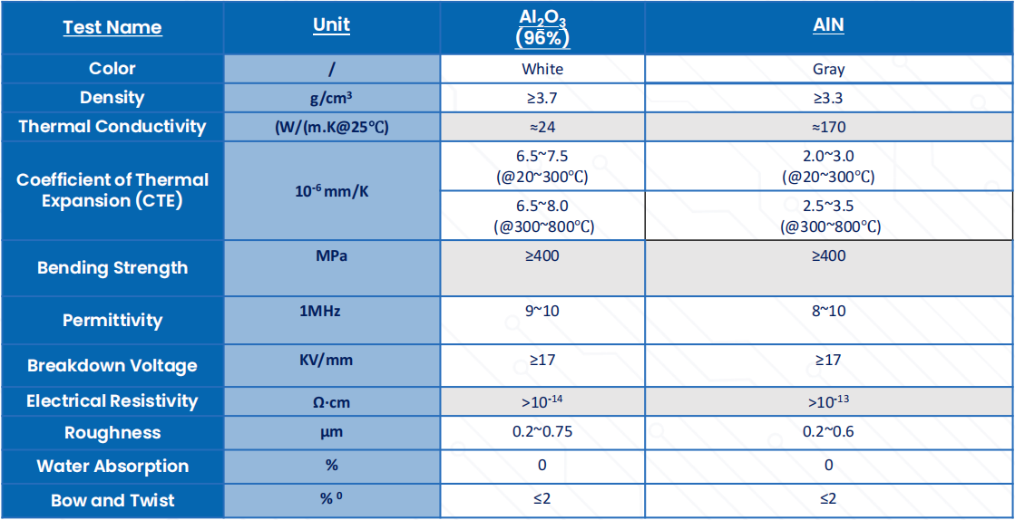
- Aluminum Nitride (AlN): Thermal Conductivity: 170-230 W/m·K. Dielectric Constant: ~8.8 @ 1MHz. Optimal for high-power, high-frequency use.
- Alumina (Al₂O₃): A robust and cost-effective standard with excellent electrical insulation properties.
Metallization & Circuit Performance:
- Technology: Direct Plated Copper (DPC).
- Copper Thickness: 10 to 100 µm.
- Circuit Resolution: Line width/spacing down to 25 µm.
- Surface Roughness: Ra < 0.1 µm.
- Peel Strength: ≥ 8 N/mm.
- Frequency Range: Suitable for applications up to 40 GHz.
Product Visualization

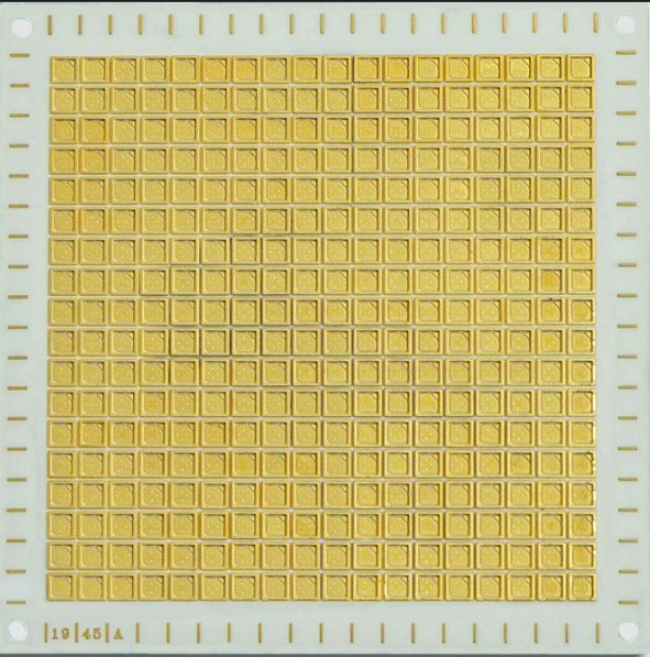
High-precision DPC substrate with fine copper traces, ready for thin film layer deposition.

Detailed comparison to guide your material selection for optimal performance and value.
Key Features & Technological Advantages
- Unparalleled Surface Quality: The ultra-smooth, mirror-like finish (Ra<0.1µm) is engineered for flawless adhesion and uniform deposition of thin film layers, a prerequisite for high-quality Film Resistor Elements and conductive paths.
- Precision Fine-Line Patterning: Achieves trace geometries down to 25µm, enabling high-density circuit designs essential for miniaturized integrated circuit packaging and advanced hybrid micro circuits.
- Superior Thermal Management: The direct bond of copper to high-thermal-conductivity ceramics like AlN creates an efficient heat spreader, crucial for cooling High power microelectronic components and laser diodes.
- High-Frequency & RF Readiness: Low-loss ceramic materials combined with precise metallization ensure excellent signal integrity, making it ideal for Microwave Components and High frequency module substrates.
- Robust Mechanical Foundation: High peel strength and dimensional stability provide a durable base for multi-layer builds and reliable operation under thermal stress.
Integration Process into Your Thin Film Fabrication
- Surface Activation: Upon receipt, perform a light plasma or chemical clean to ensure optimal surface energy for the first thin film layer.
- Thin Film Deposition: Proceed with your standard sputtering, evaporation, or CVD processes to deposit conductive, resistive, or dielectric films directly onto our prepared surface.
- Circuit Patterning: Use photolithography and etching to define your precise circuit patterns on the deposited thin films.
- Component Assembly: Mount active dies, passives, or other Bare Ceramic Plates using soldering, epoxy, or wire bonding techniques.
- Testing & Packaging: Conduct final electrical validation and proceed with encapsulation or hermetic sealing as required by your application.
Primary Application Scenarios
- RF & Microwave Communications: Power amplifiers, low-noise amplifiers (LNAs), filters, and antenna modules for telecommunications and radar systems.
- High-Power & Automotive Electronics: Substrates for Power Devices, IGBT drivers, and engine control units (ECUs) where thermal cycling and reliability are paramount.
- Aerospace & Defense Electronics: Critical for avionics, radar, and satellite communications equipment demanding high reliability in extreme environments.
- Medical & Sensor Systems: Used in implantable devices, diagnostic equipment, and high-precision sensors where signal purity and stability are non-negotiable.
- Advanced Optoelectronics: Serving as a stable platform for laser diode arrays and high-brightness LED packaging, effectively managing the associated heat.
Value Proposition for Industrial Buyers
- Increase Manufacturing Yield: Superior surface quality reduces thin film defects, directly improving your production success rate and reducing scrap.
- Enable Next-Generation Designs: Fine-line capability allows for greater circuit density and miniaturization, giving your products a competitive edge.
- Enhance End-Product Reliability: Excellent thermal and mechanical properties lead to longer operational lifespans and reduced field failures.
- Simplify System Architecture: Outstanding inherent thermal conductivity can reduce or eliminate the need for complex secondary cooling, lowering overall system cost and size.
Quality Certifications & Compliance
Our manufacturing is governed by an ISO 9001:2015 certified Quality Management System. We ensure full compliance with RoHS and REACH directives, and our processes guarantee material traceability and batch-to-batch consistency, supporting your global market requirements.
Customization & OEM/ODM Services
We provide tailored solutions to meet your specific technical and design needs:
- Material Selection: Choose between standard Al₂O₃ or high-performance AlN陶瓷基板 (AlN Ceramic Substrate).
- Dimensions & Form Factor: Custom sizes and shapes, including large panel formats for efficient batch processing.
- Circuit Layout: Full support for custom, complex circuit patterns based on your provided Gerber files.
- Advanced Features: Implementation of plated through-holes (PTH), blind vias, or cavity structures for 3D packaging.
- Surface Finish: Options include bare copper, ENIG, or immersion silver to suit your assembly process.
Manufacturing Process & Quality Assurance

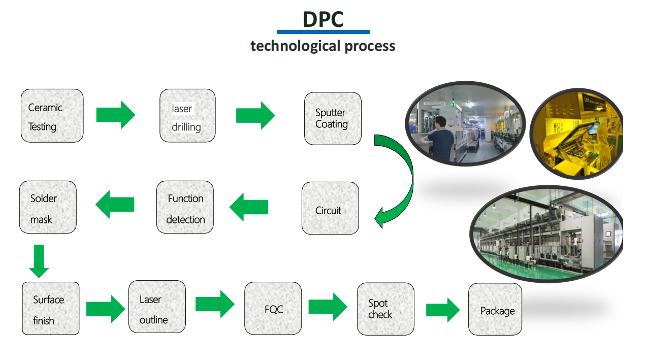
Our controlled, step-by-step manufacturing process ensures precision and reliability.
- Ceramic Substrate Preparation: High-purity ceramic blanks are precision ground and polished to achieve the required surface finish.
- Seed Layer Deposition: A thin, uniform adhesion layer is applied via sputtering.
- Patterned Copper Plating: Copper is electroplated to precise thicknesses through a photoresist mask that defines your custom circuit pattern.
- Final Etching & Finishing: The resist is removed, and the substrate undergoes final cleaning and surface treatment.
- Comprehensive QC: Each substrate undergoes 100% electrical testing, automated optical inspection (AOI), and dimensional verification before shipment.
This meticulous process, informed by our extensive experience in producing Electronic Packaging solutions, guarantees a substrate that performs as promised in your most demanding thin film applications.
Similar Video Recommendation
If you are interested in the product, contact Bossgoovideo.com for more information
- *To:
- Shaanxi Puwei Electronic Technology Co., Ltd
- *Message:
-
Submit
Main Product:
Alumina Ceramic Substrates,
Aluminum Nitride Substrates ,
Metallized Ceramics,
AlN Ceramics Disc,
DPC Substrate,
DBC Ceramic Substrate


