
Aluminum Nitride Ceramic Baseplate
2 year ago
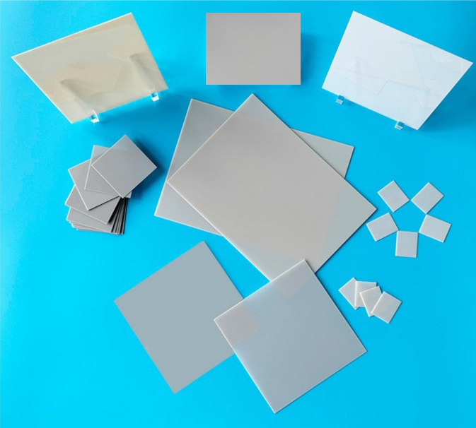
Aluminum Nitride (AlN) Ceramic Substrate
Puwei's Aluminum Nitride Ceramic Substrates represent the pinnacle of thermal management for high-performance electronic systems. Manufactured using precision casting technology and vertical integration, these substrates deliver exceptional thermal conductivity (≥175 W/m·K) combined with superior electrical insulation. They are the preferred foundation for demanding applications in electronic packaging, power devices, and high-frequency modules. Our rigorous quality control, from raw material processing to finished ceramic components, ensures consistent, reliable performance for your most critical designs.
Technical Specifications
Engineered for precision and performance, our AlN substrates meet the strict demands of microelectronics packaging and high-reliability systems.
- Material: High-purity Aluminum Nitride (AlN)
- Thermal Conductivity: Standard grade ≥175 W/m·K | Premium grade ≥200 W/m·K
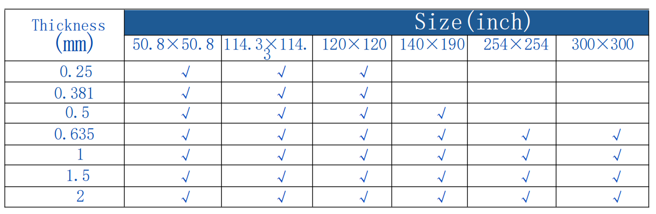
- Thickness Range: 0.10 mm to 1.5 mm (precision down to 0.10 mm)
- Electrical Properties: Volume resistivity >10¹⁴ Ω·cm, Dielectric strength >15 kV/mm
- Mechanical Strength: Flexural strength >300 MPa
- Temperature Range: -50°C to 400°C
- CTE: 4.5×10⁻⁶/K (closely matched to silicon)
- Surface Finish: Ra ≤ 0.4 μm (polished option available)
- Size Capability: Up to 150×200 mm
These properties ensure reliable performance as insulation elements and heat spreaders in integrated circuit and high-power microelectronic component applications.
Product Features & Competitive Advantages
Exceptional Thermal Management
With thermal conductivity up to 200 W/m·K (5-8x higher than alumina), our substrates efficiently dissipate heat from high-density power devices and microwave components, preventing thermal runaway and significantly extending device lifespan.
Versatile Metallization Compatibility
Engineered to support DPC, DBC, AMB, thick film, and thin film printing processes. This offers maximum design flexibility for creating RF circuits, thick film hybrid microcircuits, and advanced thermoelectric cooling assemblies.
Precision Manufacturing & Customization
Advanced casting technology ensures tight dimensional tolerances and superior surface quality. We offer customized thicknesses (down to 0.10 mm), surface finishes, and sizes, ideal for specialized sensor packaging and demanding optoelectronics applications.
Superior Electrical Insulation
High dielectric strength (>15 kV/mm) and volume resistivity make it an excellent insulation element, ensuring safety and signal integrity in high-voltage environments and dense microelectronics packaging.
Integration Roadmap: From Specification to Production
A structured approach to incorporating Puwei AlN substrates into your designs for optimal performance.
- Design Consultation: Collaborate with our engineers to define critical substrate parameters—thermal budget, electrical isolation needs, and mechanical constraints.
- Metallization & Patterning Selection: Choose the optimal technique (DPC for fine features, DBC/AMB for high power, thick/thin film for integrated passives) based on your circuit design and assembly process.
- Surface & Dimensional Specification: Define surface finish (as-fired, ground, or polished) and precise dimensions to ensure optimal component attachment and system fit.
- Prototyping & Thermal Validation: Utilize samples to validate thermal performance, CTE matching, and reliability under your specific operating conditions.
- Volume Integration & QA: Scale to production with our lot traceability and consistent quality, performing in-house verification of key parameters.
Primary Application Scenarios
Power Electronics & Semiconductor Devices
Ideal for IGBT modules, power converters, and inverters. Serves as a critical insulation element and heat spreader, enhancing the reliability of high-power microelectronic components in EV, industrial, and renewable energy systems.
RF & Microwave Communication
Provides low dielectric loss and stable thermal performance for high-frequency modules, microwave applications, and RF power amplifiers used in 5G infrastructure and radar systems.
Advanced Electronics & Sensor Packaging
Critical for microelectronics packaging, sensor packaging, and thermoelectric semiconductor module plates, enabling miniaturization while maintaining superior thermal control.
Optoelectronics & High-Power LED Systems
Used as a high-efficiency heat sink substrate for laser diodes, high-power LEDs, and other optoelectronics applications where junction temperature directly impacts light output and lifetime.
Value Proposition for Your Business
- Extended Component Life: Superior heat dissipation reduces thermal stress, significantly increasing the lifespan of sensitive semiconductors and assemblies.
- Increased Power Density: Enables more compact, higher-power designs by efficiently managing heat in smaller footprints.
- Reduced System Costs: Minimizes or eliminates the need for complex external cooling systems, lowering BOM and assembly costs.
- Enhanced Field Reliability: Excellent material stability and CTE matching ensure consistent performance in harsh thermal cycling environments, reducing failure rates.
- Design Freedom: Comprehensive customization and metallization options allow for optimized, application-specific electronic packaging solutions.
Customization & OEM Services
Puwei provides extensive customization to ensure our AlN substrates precisely match your technical requirements and simplify your assembly process for ceramic chips and complex modules.
- Dimensions & Tolerances: Custom sizes up to 150×200 mm and thicknesses from 0.10 mm, with tight tolerances.
- Surface Finish: As-fired, precision ground, or polished surfaces with controlled Ra values.
- Metallization & Patterning: DPC, DBC, AMB, thick film, or thin film printing with custom circuit patterns.
- Material Grades: Tailored formulations for enhanced bending strength or maximized thermal conductivity.
- Special Features: Laser marking, precision through-holes/vias, and specific edge profiling available.
Production Process & Quality Assurance
Our manufacturing excellence is built on a vertically integrated, tightly controlled process, ensuring that every substrate functions as a reliable ceramic component.
- High-Purity Powder Formulation: Precise mixing of AlN with sintering aids for optimal densification.
- Precision Casting & Forming: Advanced tape casting or dry pressing for uniform green sheets.
- Controlled Sintering: High-temperature profile in nitrogen atmosphere to achieve >99% theoretical density.
- Precision Grinding & Finishing: Surface planarization and thickness control to customer specifications.
- Comprehensive Inspection: 100% dimensional, thermal conductivity sampling, and dielectric strength testing.
- Clean Packaging: Anti-static, dust-free packaging for safe transit and direct use in cleanroom environments.
Statistical Process Control (SPC) ensures exceptional batch-to-batch consistency, making Puwei a trusted partner for high-reliability applications.
Certifications & Compliance
Manufactured in ISO 9001:2015 certified facilities. Our quality management system ensures full traceability and adherence to international standards. All materials are RoHS and REACH compliant, meeting global environmental and safety requirements for electronic components.
Similar Video Recommendation


If you are interested in the product, contact Bossgoovideo.com for more information
- *To:
- Shaanxi Puwei Electronic Technology Co., Ltd
- *Message:
-
Submit
Main Product:
Alumina Ceramic Substrates,
Aluminum Nitride Substrates,
Metallized Ceramics,
AlN Ceramics Disc ,
DPC Substrate,
DBC Ceramic Substrate