
Electronic Metallized Ceramic Substrate
2 year ago
Electronic Metallized Ceramic Substrates: Advanced Platform for High-Reliability Electronics
Product Overview
Puwei's Electronic Metallized Ceramic Substrates are engineered to solve the core challenges of modern electronics: heat dissipation, electrical isolation, and mechanical reliability. By seamlessly integrating high-performance ceramics (Alumina, AlN, BeO) with robust Mo/Mn or Tungsten (W) metallization, we create a versatile platform that serves as the structural and functional backbone for your most demanding applications. This technology is fundamental to advanced Electronic Packaging and Microelectronics Packaging, providing the essential link between sensitive semiconductor dies and the larger system.
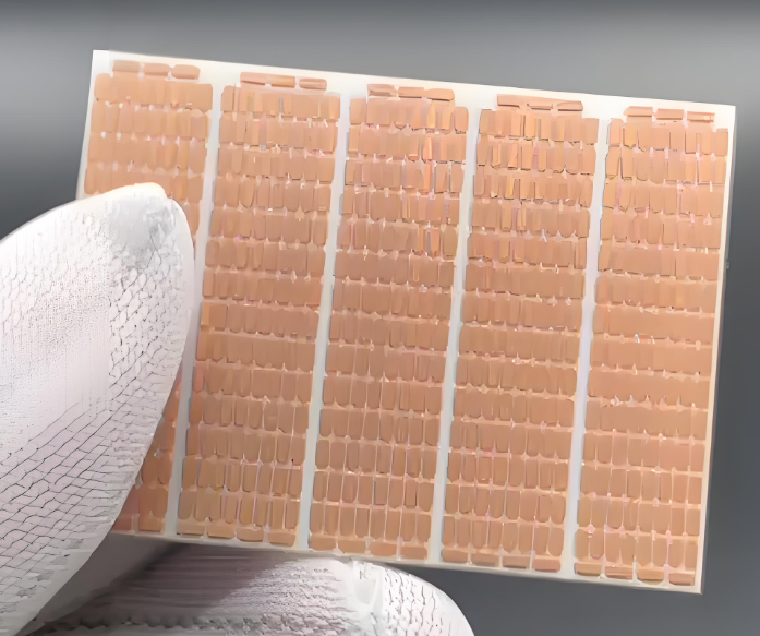
High-precision metallized ceramic substrate enabling reliable component integration and thermal management.
Core Value for Engineering & Procurement
- Solve Thermal Runaway in Dense Designs: Our substrates act as efficient heat spreaders, drawing heat away from high-power microelectronic components and power devices, enabling higher power density and preventing performance throttling.
- Ensure Signal Integrity and Isolation: The ceramic base provides excellent dielectric properties, preventing crosstalk and leakage, which is critical for high-frequency modules and RF circuits.
- Achieve Unmatched Mechanical & Thermal Durability: The metallurgical bond created by our Mo/Mn or W processes withstands severe thermal cycling and mechanical vibration, ensuring long-term reliability in automotive and industrial environments.
- Simplify Supply Chain with a Integrated Solution: Combine insulation, conduction, and thermal management into one certified component, reducing assembly steps and qualifying multiple vendors.
- Optimize Cost with Material Choice: Select from cost-effective Alumina for standard applications or high-conductivity AlN for extreme thermal needs, ensuring the best price-to-performance ratio for your project.
Technical Specifications & Material Options
Ceramic Material Portfolio
We offer a range of ceramic bases to match your specific thermal, electrical, and cost requirements. Options include various grades of Alumina Ceramic Substrate (Al2O3) (94% to 99.6% purity), high thermal conductivity Aluminum Nitride (AlN, 170-230 W/m·K), and premium-performance Beryllium Oxide (BeO). We also develop custom formulations for specialized needs.
Metallization & Performance
Our core expertise lies in Mo/Mn and Tungsten (W) paste metallization, fired to create a strong, hermetic bond with the ceramic. This provides excellent brazing compatibility, high adhesion strength, and a superior surface for subsequent plating or component attachment. Key characteristics include high dielectric strength, matched Coefficient of Thermal Expansion (CTE) to semiconductors, and outstanding flexural strength.
Key Features & Technology Advantages
Unlike simple circuit boards, our metallized substrates are integral to module performance. The ceramic provides electrical isolation and structural support, while the patterned metal layer facilitates electrical interconnection and acts as a primary heat conduction path. This is especially critical for insulation elements in high-voltage applications and thermal management in thermoelectric cooling assemblies.
- Proven Metallization Technology: Mo/Mn and W processes offer superior bond strength and high-temperature stability compared to many thin-film alternatives.
- Tailored Thermal Pathway Design: The metal layer can be optimized to channel heat efficiently away from hot spots, directly impacting the reliability of integrated circuit and power modules.
- Foundation for Hybrid Circuits: The surface is ideal for depositing additional thick-film layers, making it the perfect platform for Thick Film Hybrid Microcircuits and hybrid micro circuits.
Integration & Assembly Guidelines
- Design & Material Selection: Define thermal, electrical (voltage, frequency), and mechanical requirements. Choose the ceramic material (Al2O3 vs. AlN) and metallization type with our engineering support.
- Substrate Fabrication: Provide your circuit layout (Gerber file) for custom metallization patterning. We manufacture the substrate to your exact dimensions and specifications.
- Pre-Assembly Preparation: Clean substrates thoroughly (e.g., plasma clean) to ensure optimal surface energy for soldering or brazing.
- Component Attachment: Use high-temperature solder or active brazing alloys (for Mo/Mn) to attach semiconductor dies, capacitors, or other components to the metal pads.
- Secondary Assembly & Testing: Complete wire bonding, attach heat sinks, and conduct rigorous electrical, thermal, and mechanical validation tests.
Primary Application Scenarios
Power Electronics & Automotive
The substrate of choice for IGBT modules, SiC/GaN power devices, and EV traction inverters. Provides critical insulation and heat spreading for high-current applications.
RF & Microwave Communications
Enables low-loss performance in microwave components, power amplifiers, and filters for 5G infrastructure, radar, and satellite systems, where signal integrity is paramount.
Optoelectronics & Sensing
Used in high-power LED packaging, laser diode mounts, and sensor packaging, where stable thermal performance ensures consistent output and longevity.
Aerospace & Defense Electronics
Provides hermetic sealing and unmatched reliability for critical avionics, radar systems, and microelectronics in extreme environments.
Industrial & Energy Systems
Found in motor drives, solar inverters, and industrial controls, offering durability and performance in harsh operational conditions.
Certifications & Quality Commitment
Puwei Ceramic operates under an ISO 9001:2015 certified quality management system. All materials and processes comply with RoHS and REACH directives. We maintain full material traceability and employ industry-standard testing protocols (adhesion pull tests, thermal cycling, electrical breakdown) to ensure every substrate, including Bare Ceramic Plates destined for assembly, meets the highest standards of performance and reliability.
Customization & OEM/ODM Services
We are a solutions partner, not just a supplier. Our comprehensive customization capabilities include:
- Full Design Freedom: Any size, shape, thickness, and complex multi-layer metallization pattern.
- Material Expertise: Guidance on selecting the optimal ceramic (Al2O3, AlN) and metallization (Mo/Mn, W) for your electrical, thermal, and budget needs.
- Value-Added Processing: Precision laser cutting, drilling of vias, and application of specific surface finishes (Ni, Au) for solderability or wire bonding.
- Co-Engineering Support: Collaborative development from prototype to volume production, leveraging our deep knowledge in Metallized Ceramics.
Manufacturing Process & Quality Control
Our production is a vertically controlled sequence: from stringent QC of incoming ceramic powder, through precision sintering and shaping, to the critical metallization steps where Mo/Mn or W paste is screen-printed and fired in controlled atmosphere furnaces. Each batch undergoes 100% inspection for dimensional accuracy, adhesion strength, and electrical properties. This rigorous process ensures we deliver a consistently reliable foundation for your most critical electronic assemblies.
Similar Video Recommendation


If you are interested in the product, contact Bossgoovideo.com for more information
- *To:
- Shaanxi Puwei Electronic Technology Co., Ltd
- *Message:
-
Submit
Main Product:
Alumina Ceramic Substrates,
Aluminum Nitride Substrates,
Metallized Ceramics,
AlN Ceramics Disc ,
DPC Substrate,
DBC Ceramic Substrate