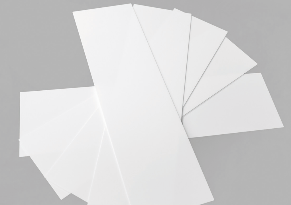
Large Size Alumina Ceramic Substrate
2 year agoLarge Size Low Warpage Alumina Ceramic Substrate
Product Overview
Puwei Ceramic delivers industry-leading alumina ceramic substrates engineered for superior performance in demanding electronic packaging applications. Our proprietary manufacturing technology enables production of exceptionally large substrates (up to 240×280×1mm) with minimal warpage under 0.25%, addressing critical challenges in microelectronics packaging and circuit integration.
These advanced electronic ceramic products provide exceptional dimensional stability, excellent electrical insulation, and superior thermal management properties. Ideal for high-frequency modules and power devices, our substrates ensure reliable performance in precision electronic assemblies.
Technical Specifications
- Material Composition: 96% Alumina Ceramic (Al₂O₃)
- Available Sizes: Standard and custom dimensions up to 240×280mm
- Thickness Range: 0.2mm to 2.00mm
- Maximum Warpage: <0.25% (significantly lower than industry standard)
- Surface Finish: Precision polished for optimal flatness
- Dimensional Tolerance: ±0.1mm to ±0.5mm
- Volume Resistivity: >10¹⁴ Ω·cm
- Dielectric Strength: >10 kV/mm
- Thermal Conductivity: 20-25 W/m·K
- Coefficient of Thermal Expansion: 7.2-8.4 × 10⁻⁶/°C
Product Images

96% Alumina Ceramic Substrate - Large Format Design

Superior Flatness Achieved Through Special Manufacturing Process

Performance Parameters of 96% Alumina Ceramic Substrate

Dimensional Tolerances for Mold Stamped Substrates

Dimensional Tolerances for Laser-Processed Substrates
Product Features & Advantages
Exceptional Flatness & Minimal Warpage
Our proprietary flat firing technique reduces camber to less than 0.25%, significantly below the 0.39% industry standard. This exceptional flatness ensures perfect alignment in integrated circuit assemblies and prevents stress in mounted components.
Advanced Iron Impurity Reduction
Unique iron removal process reduces iron content inclusions by over 95%, eliminating red spots that compromise appearance and electrical properties. This ensures superior volume resistivity and dielectric strength for microwave applications.
Large Format Manufacturing Capability
We specialize in extra-large substrates (up to 240×280×1mm) that are difficult to source elsewhere, making us the preferred supplier for applications requiring substantial circuit real estate in thick film hybrid microcircuits.
Precision Dimensional Control
Whether mold-stamped or laser-processed, our substrates maintain tight dimensional tolerances critical for automated assembly processes, reducing integration issues and improving manufacturing yield.
Superior Electrical Performance
High volume resistivity (>10¹⁴ Ω·cm) and exceptional dielectric strength (>10 kV/mm) make our substrates ideal for RF circuits and high-voltage applications where insulation integrity is paramount.
Implementation Guide
- Design Consultation: Collaborate with our engineering team during design phase to optimize substrate specifications
- Material Selection: Choose between standard 96% alumina or explore enhanced material options
- Fabrication Method: Select appropriate method (mold stamping or laser processing) based on tolerance requirements
- Surface Preparation: Specify required surface treatments or metallization patterns
- Integration Planning: Plan assembly considering thermal expansion characteristics
- Quality Verification: Implement inspection protocols to verify dimensional accuracy
Application Scenarios
Power Electronics & Semiconductor Packaging
Our large-format, low-warpage substrates excel in power modules, IGBTs, and automotive power systems where flatness ensures proper thermal management and reliability for high-power microelectronic components.
LED & Optoelectronics Systems
Exceptional dimensional stability makes our substrates perfect for high-density LED arrays and display backplanes where precise component placement is critical in optoelectronics applications.
RF and Microwave Circuits
Low dielectric loss and consistent electrical properties across large areas make our substrates valuable for microwave components requiring stable performance at high frequencies.
Semiconductor Test Equipment
Thermal stability and flatness ensure reliable performance in demanding test environments where temperature cycling can cause conventional substrates to fail.
Medical Imaging Systems
For X-ray detectors, ultrasound systems, and other medical imaging applications, our substrates provide the reliability and precision required in medical electronics, serving as excellent insulation elements.
Customer Benefits
- Improved Manufacturing Yield: Reduced warpage means fewer assembly issues and higher production yields
- Enhanced Product Reliability: Superior materials and manufacturing extend product lifespan
- Design Flexibility: Large format capability enables innovative product designs
- Reduced Total Cost: Fewer rejects and less rework translate to lower overall costs
- Technical Expertise: Access to engineering support for design optimization
- Supply Chain Security: Reliable supply from certified manufacturer with significant capacity
Certifications and Quality Compliance
Our manufacturing facilities and processes are certified to international quality standards (Certificate: GXLH41023Q10642R0S). We maintain rigorous quality control throughout production to ensure consistent performance and reliability for all ceramic components.
Our alumina ceramic substrates comply with relevant industry standards for electronic ceramics and are suitable for automotive, medical, and industrial applications requiring certified components.
Customization Services
We offer comprehensive OEM & ODM services to meet specific customer requirements. Our technical team can produce ceramic substrates with thicknesses from 0.2mm to 2.00mm, with custom dimensions and geometries available.
Our expertise extends to specialized requirements including custom metallization patterns, vias, and cavities. We provide metallized ceramics with various metal coatings (Cu, Al, Au, Ag) optimized for specific application needs in sensor packaging and other specialized fields.
Production Process & Quality Assurance
Our manufacturing incorporates advanced techniques developed specifically for large-format, low-warpage substrates:
- Material Preparation: High-purity alumina powder with proprietary iron reduction
- Tape Casting: Precision controlled process for uniform thickness
- Special Flat Firing: Proprietary technique minimizing warpage and camber
- Precision Machining: Mold stamping or laser processing per tolerance requirements
- Surface Finishing: Precision polishing and cleaning for optimal quality
- Rigorous Inspection: 100% dimensional verification and electrical testing
Each production batch undergoes multiple quality checkpoints to ensure dimensional accuracy, surface quality, and electrical performance for all ceramic chips and substrates.
Similar Video Recommendation
If you are interested in the product, contact Bossgoovideo.com for more information
- *To:
- Shaanxi Puwei Electronic Technology Co., Ltd
- *Message:
-
Submit
Main Product:
Alumina Ceramic Substrates,
Aluminum Nitride Substrates,
Metallized Ceramics ,
AlN Ceramics Disc,
DPC Substrate,
DBC Ceramic Substrate


