
Aluminum Nitride Ceramic Substrate for Electronic Packaging
2 year ago
Laser Precision Machining Services for Aluminum Nitride (AlN) Substrates
Puwei delivers micron-level precision for advanced Electronic Packaging and high-frequency applications with our state-of-the-art UV and fiber laser machining services for high-purity Aluminum Nitride substrates.

Why Choose Laser Precision Machining for AlN?
- Micron-Level Accuracy: Achieve features as fine as 10μm with ±2μm positioning accuracy.
- Non-Contact Process: Eliminates mechanical stress, tool wear, and substrate damage.
- Complex Design Freedom: Create intricate geometries impossible with conventional methods.
- Preserves Material Integrity: Minimal heat-affected zone protects AlN's superior thermal and electrical properties.
- Rapid Prototyping to Production: Accelerate your development cycle for Microelectronics Packaging.
Technical Specifications & Capabilities
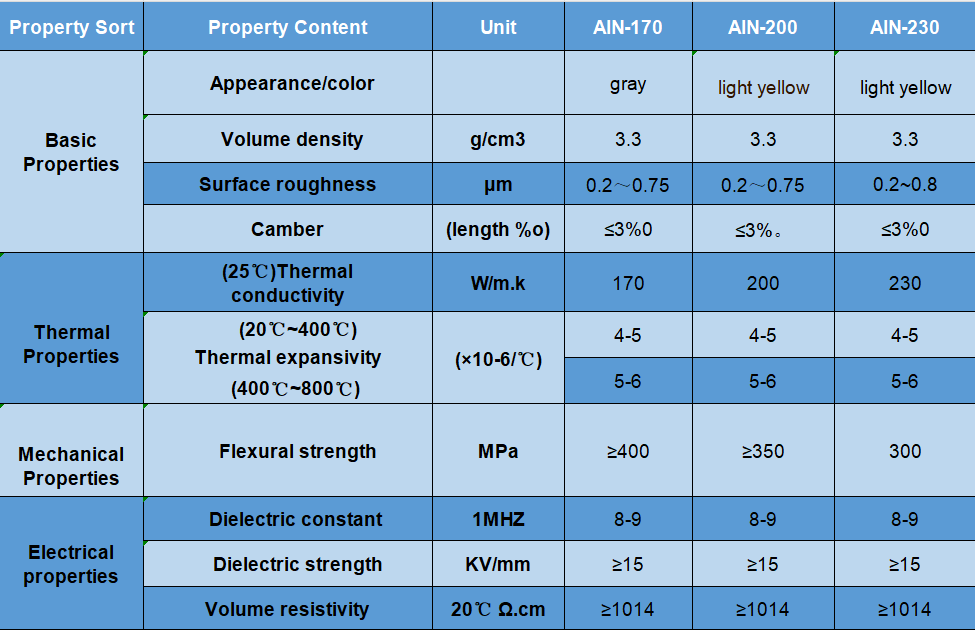
Material Properties
Base Material: High-Purity Aluminum Nitride (AlN). Thermal Conductivity: Standard ≥175W/m·K, High-grade ≥200W/m·K. Dielectric Strength: 15-20 kV/mm. Thermal Expansion: 4.5-5.5 ppm/°C (RT-400°C).
Laser Machining Parameters
Minimum Feature: 10μm. Positioning Accuracy: ±2μm. Surface Roughness: Ra ≤ 0.4μm. Thickness Range: 0.10mm - 3.0mm. Max Substrate Size: 150mm × 150mm.
Laser Processes Offered
- Laser Ablation & Micro-structuring: For fine grooves and channels in Sensor packaging.
- Precision Laser Cutting: Clean edges for High frequency module substrates.
- Laser Drilling & Via Formation: High-density interconnects for Microwave Applications.
Key Applications for Laser-Machined AlN Substrates
Our services enable next-generation performance in critical industries:
- Power Electronics & RF/Microwave: Ideal for Power Devices, Microwave Components, and RF circuits requiring superior thermal management and signal integrity.
- Advanced Optoelectronics: Precision features for laser diode mounts, optical alignment, and Optoelectronics Applications.
- MEMS & Advanced Sensor Systems: Create intricate microstructures with high dimensional stability.
- High-Density Integrated Circuit Packaging: Enables fine-pitch interconnects and advanced thermal structures for 3D packaging and system-in-package (SiP).
Your Project Implementation Steps
- Design & Feasibility Review: We analyze your requirements for manufacturability.
- CAD Programming & Fixture Design: Preparing for precise laser processing.
- Laser Parameter Optimization: Fine-tuning for your specific AlN material and design.
- Precision Machining & Quality Inspection: Automated processing followed by rigorous 100% dimensional inspection.
- Post-Processing & Delivery: Final cleaning and documentation for traceability.
Business Value for OEMs & Design Engineers
- Enhance Performance: Up to 50% better heat dissipation enables higher power density and extends device lifetime.
- Reduce Costs: Precision features minimize assembly rework and can reduce external cooling requirements.
- Accelerate Innovation: Rapid prototyping allows faster iteration for complex Microelectronics designs.
- Ensure Quality & Consistency: ISO 9001:2015 certified processes and statistical process control deliver high yield and reliability.
Customization & Quality Assurance
Puwei offers tailored solutions to meet exact application needs:
- Material & Geometry: Choose thermal conductivity grade, thickness (0.10-3.0mm), and custom shapes.
- Surface Finish & Metallization: Options include as-fired, ground, or polished surfaces, compatible with DBC, DPC, AMB processes.
- End-to-End Quality Control: From raw material verification to final inspection, ensuring every substrate meets stringent specifications for high-reliability applications.
Technical FAQ
Q: Why laser machining over mechanical methods for AlN?
A: Laser processing provides non-contact, stress-free machining with micron precision, preserving the intrinsic properties of brittle AlN ceramic—critical for advanced Electronic Packaging.
Q: What makes AlN superior for thermal management?
A: AlN offers high thermal conductivity (175-200 W/m·K) combined with excellent electrical insulation and CTE matching to silicon, making it ideal for high-power and Microwave Applications.
Puwei's Laser Precision Machining Service transforms high-purity Aluminum Nitride into performance-critical components. Combining advanced material science with precision laser technology, we empower your innovations in power electronics, high-frequency systems, and advanced packaging with reliability, precision, and design flexibility.
Similar Video Recommendation


If you are interested in the product, contact Bossgoovideo.com for more information
- *To:
- Shaanxi Puwei Electronic Technology Co., Ltd
- *Message:
-
Submit
Main Product:
Alumina Ceramic Substrates,
Aluminum Nitride Substrates,
Metallized Ceramics,
AlN Ceramics Disc,
DPC Substrate ,
DBC Ceramic Substrate